

Gerber files are important data used by PCB manufacturers to produce circuit boards exactly according to the original design. These files contain information such as copper layers, solder mask layers, silkscreen and drilling positions. However, if Gerber files are incorrect or missing data, the manufacturing process can encounter serious issues. Therefore, checking Gerber files before production is a very important step.
In this article, let’s explore what Gerber files are and the common errors that can affect the PCB manufacturing process.
1. What is a Gerber file?
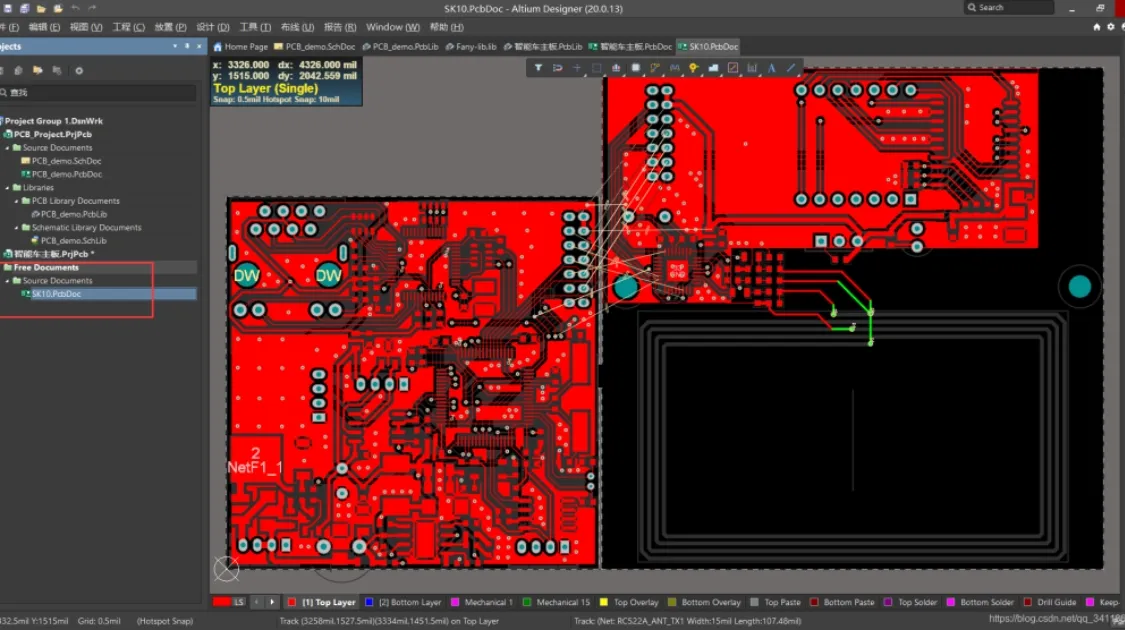
A Gerber file is a standard data format used in PCB design and manufacturing. It transfers the complete design information from PCB design software to the manufacturing factory, ensuring that the circuit board is produced exactly as intended.
A typical Gerber file includes important data such as:
- Copper layers.
- Solder mask layers.
- Silkscreen.
- Drill file.
- Board outline.
PCB manufacturers use Gerber files to review the design, prepare production data and operate PCB fabrication machines. If a Gerber file is missing or contains incorrect information, the production process may encounter errors or require revisions before manufacturing can begin.
2. How important are Gerber files in PCB manufacturing?
Gerber files play a crucial role in the PCB manufacturing process as they serve as the primary input data for fabricating the circuit board. All production steps such as copper layer formation, drilling, solder mask application and silkscreen printing are based on the information provided in Gerber files.
In addition, Gerber files help manufacturers accurately understand the PCB design created by engineers. If the data is missing or incorrect, the finished board may have serious issues such as incorrect dimensions, misaligned drill holes or short circuits.
Therefore, the quality of Gerber files directly affects the accuracy, stability and overall quality of the final PCB after production.
3. Common Gerber file errors
During the Gerber file export process, many different types of errors can occur, not limited to a few specific cases. These issues may come from the design stage, the file export process or CAD software configuration.
Below are some common Gerber file errors in PCB manufacturing:
3.1. Missing or incorrect layers
This is one of the most common errors when exporting Gerber files. Typical cases include missing copper layers, solder mask layers or silkscreen layers. In addition, unclear layer naming can also cause confusion for manufacturers during data processing.
If a layer is missing or incorrect, the fabricated PCB may not match the original design, which directly affects board quality.
3.2. Incorrect drill files
Drill files define the position and size of holes on the PCB. These files are usually transferred directly to CNC machines for drilling.
If the drill file is missing, has an incorrect format or does not match the PCB design, manufacturers may face difficulties when importing production data. This can lead to incorrect hole positions, wrong hole sizes or issues during component assembly.
Common drill file formats include .drl, .xln or NC Drill files exported directly from PCB design software.
3.3. Incorrect PCB size or outline
The board outline defines the physical shape and size of the PCB during manufacturing. Manufacturers rely on this data for board cutting, PCB positioning and mechanical processing.
If the board outline is incorrect, not closed or does not match the design, the final PCB may not fit the mechanical enclosure or related components. In some cases, this error may even cause production to pause for design verification.
Therefore, checking PCB size and shape carefully before exporting Gerber files is very important to avoid manufacturing issues.
3.4. Solder mask and silkscreen errors
Solder mask and silkscreen are important PCB layers that support component soldering, identification and post-production inspection.
Common issues include text overlapping pads, incorrect solder mask clearance or unclear component markings. These problems can make soldering, inspection and PCB assembly more difficult.
In addition, incorrect solder mask design may increase the risk of short circuits or reduce PCB reliability during operation.
3.5. Incorrect units or file scale
Incorrect units or scaling can seriously affect the entire PCB manufacturing process. Common cases include mixing up millimeters and inches or exporting files with incorrect scaling.
When this happens, the PCB may be scaled incorrectly compared to the original design. This affects not only the board shape but also component positions, drill holes and trace spacing.
To avoid production issues, it is important to carefully check units and scaling before exporting Gerber files and sending them to the PCB manufacturer.
3.6. Copper too close to board edge
The distance between copper layers and the PCB edge is an important factor in design and manufacturing. If copper is placed too close to the edge, PCB cutting or routing may expose the copper layer.
This increases the risk of short circuits, board damage or reduced PCB stability during operation. This issue usually occurs when the design does not follow standard manufacturing clearance rules.
Therefore, it is necessary to ensure proper clearance between copper and the PCB edge before exporting Gerber files to minimize manufacturing risks.
4. How PCB manufacturers check Gerber files
Before starting PCB production, manufacturers usually inspect Gerber files to identify errors that could affect the fabrication process. This is an important step that helps reduce production defects and avoid data corrections during manufacturing.
Common inspection items include:
- Verifying all layers and drill files are complete.
- Checking PCB dimensions and board outline consistency.
- Inspecting clearance between copper traces and other elements.
- Confirming manufacturability before production begins.
In addition, many manufacturers also use Gerber viewer software or DFM tools to review design data before proceeding with PCB fabrication.
5. Things to check before sending Gerber files
Before sending Gerber files to a PCB manufacturer, it is important to carefully review the design data to minimize production errors. Proper pre-checking helps reduce the risk of mistakes, avoid delays and prevent data revisions after manufacturing has started.
Key items to check include:
- Ensuring all required layers are included such as copper layers, solder mask and silkscreen.
- Checking drill files to confirm correct hole positions and sizes.
- Verifying PCB board outline and actual dimensions.
- Ensuring proper clearance between copper traces and board edges according to manufacturing capability.
- Using clear file and layer naming to avoid confusion during data processing.
- Reviewing the entire design using a Gerber viewer before sending to the PCB manufacturer.
In addition, many companies also perform DFM checks to evaluate PCB manufacturability and detect issues that could affect the fabrication process.
Conclusion
Gerber files play an important role in PCB manufacturing as they allow factories to fabricate circuit boards according to the original design. However, if the files are missing or contain incorrect data, the PCB may experience various issues during production and assembly.
Therefore, carefully checking Gerber files before sending them to the manufacturer is a necessary step to reduce errors, optimize production timelines and ensure PCB quality.